| Listing 1 - 4 of 4 |
Sort by
|
Book
ISBN: 0792337093 940104189X 9401104239 9780792337096 Year: 1995 Volume: 300
Abstract | Keywords | Export | Availability | Bookmark
 Loading...
Choose an application
- Reference Manager
- EndNote
- RefWorks (Direct export to RefWorks)
Book
ISBN: 0883188163 9780883188163 Year: 1992 Volume: 241
Abstract | Keywords | Export | Availability | Bookmark
 Loading...
Choose an application
- Reference Manager
- EndNote
- RefWorks (Direct export to RefWorks)
537.533.35 <063> --- Scanning probe microscopy --- -Scanning tunneling microscopy --- -#WSCH:MODS --- STM (Microscopy) --- Scanned probe microscopy --- Scanning electron microscopy --- 537.533.35 <063> Electron microscopy--Congressen --- Electron microscopy--Congressen --- Congresses --- Scanning tunneling microscopy --- #WSCH:MODS --- Scanning probe microscopy - Congresses. --- Scanning tunneling microscopy - Congresses. --- Scanning tunneling microscopy - Congresses --- Scanning probe microscopy - Congresses

ISBN: 0792359402 0792359399 9401144516 Year: 1999 Publisher: Dordrecht ; Norwell, MA : Kluwer,
Abstract | Keywords | Export | Availability | Bookmark
 Loading...
Choose an application
- Reference Manager
- EndNote
- RefWorks (Direct export to RefWorks)
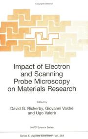
The Advanced Study Institute provided an opportunity for researchers in universities, industry and National and International Laboratories, from the disciplines ofmaterials science, physics, chemistry and engineering to meet together in an assessment of the impact of electron and scanning probe microscopy on advanced material research. Since these researchers have traditionally relied upon different approaches, due to their different scientific background, to advanced materials problem solving, presentations and discussion within the Institute sessions were initially devoted to developing a set ofmutually understood basic concepts, inherently related to different techniques ofcharacterization by microscopy and spectroscopy. Particular importance was placed on Electron Energy Loss Spectroscopy (EELS), Scanning Probe Microscopy (SPM), High Resolution Transmission and Scanning Electron Microscopy (HRTEM, HRSTEM) and Environmental Scanning Electron Microscopy (ESEM). It was recognized that the electronic structure derived directly from EELS analysis as well as from atomic positions in HRTEM or High Angle Annular Dark Field STEM can be used to understand the macroscopic behaviour of materials. The emphasis, however, was upon the analysis of the electronic band structure of grain boundaries, fundamental for the understanding of macroscopic quantities such as strength, cohesion, plasticity, etc.
Electron microscopy --- Congresses --- Scanning probe microscopy --- Materials research --- Materials science. --- Physical chemistry. --- Condensed matter. --- Materials—Surfaces. --- Thin films. --- Inorganic chemistry. --- Characterization and Evaluation of Materials. --- Physical Chemistry. --- Condensed Matter Physics. --- Surfaces and Interfaces, Thin Films. --- Inorganic Chemistry. --- Inorganic chemistry --- Chemistry --- Inorganic compounds --- Films, Thin --- Solid film --- Solid state electronics --- Solids --- Surfaces (Technology) --- Coatings --- Thick films --- Condensed materials --- Condensed media --- Condensed phase --- Materials, Condensed --- Media, Condensed --- Phase, Condensed --- Liquids --- Matter --- Chemistry, Theoretical --- Physical chemistry --- Theoretical chemistry --- Material science --- Physical sciences --- Electron microscopy. --- Scanning probe microscopy. --- Materials --- Microscopy. --- Microscopy --- Scanned probe microscopy --- Scanning electron microscopy

ISBN: 1402030177 1402030185 9786610263707 1280263709 1402030193 Year: 2005 Volume: 186 Publisher: Dordrecht : Springer Netherlands : Imprint: Springer,
Abstract | Keywords | Export | Availability | Bookmark
 Loading...
Choose an application
- Reference Manager
- EndNote
- RefWorks (Direct export to RefWorks)
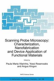
As the characteristic dimensions of electronic devices continue to shrink, the ability to characterize their electronic properties at the nanometer scale has come to be of outstanding importance. In this sense, Scanning Probe Microscopy (SPM) is becoming an indispensable tool, playing a key role in nanoscience and nanotechnology. SPM is opening new opportunities to measure semiconductor electronic properties with unprecedented spatial resolution. SPM is being successfully applied for nanoscale characterization of ferroelectric thin films. In the area of functional molecular materials it is being used as a probe to contact molecular structures in order to characterize their electrical properties, as a manipulator to assemble nanoparticles and nanotubes into simple devices, and as a tool to pattern molecular nanostructures. This book provides in-depth information on new and emerging applications of SPM to the field of materials science, namely in the areas of characterisation, device application and nanofabrication of functional materials. Starting with the general properties of functional materials the authors present an updated overview of the fundamentals of Scanning Probe Techniques and the application of SPM techniques to the characterization of specified functional materials such as piezoelectric and ferroelectric and to the fabrication of some nano electronic devices. Its uniqueness is in the combination of the fundamental nanoscale research with the progress in fabrication of realistic nanodevices. By bringing together the contribution of leading researchers from the materials science and SPM communities, relevant information is conveyed that allows researchers to learn more about the actual developments in SPM applied to functional materials. This book will contribute to the continuous education and development in the field of nanotechnology.
Materials --- Scanning probe microscopy --- Matériaux --- Microscopie à sonde à balayage --- Microscopy --- Congresses. --- Congresses --- Microbiologie --- Congrès --- Materials - Microscopy - Congresses. --- Scanning probe microscopy. --- Atomic Physics --- Materials Science --- Physics --- Chemical & Materials Engineering --- Engineering & Applied Sciences --- Physical Sciences & Mathematics --- Scanning electron microscopy --- Matériaux --- Microscopie à sonde à balayage --- Congrès --- EPUB-LIV-FT LIVPHYSI SPRINGER-B --- Scanned probe microscopy --- Physics. --- Condensed matter. --- Optical materials. --- Electronic materials. --- Nanotechnology. --- Thin films. --- Condensed Matter Physics. --- Optical and Electronic Materials. --- Surfaces and Interfaces, Thin Films. --- Surfaces. --- Electron microscopy --- Surfaces (Physics). --- Surface chemistry --- Surfaces (Technology) --- Molecular technology --- Nanoscale technology --- High technology --- Optics --- Materials—Surfaces. --- Films, Thin --- Solid film --- Solid state electronics --- Solids --- Coatings --- Thick films --- Electronic materials --- Condensed materials --- Condensed media --- Condensed phase --- Materials, Condensed --- Media, Condensed --- Phase, Condensed --- Liquids --- Matter --- Surface phenomena --- Friction --- Surfaces (Physics) --- Tribology --- Surfaces
| Listing 1 - 4 of 4 |
Sort by
|

 Search
 Feedback
 About
About Help
Help News
News