| Listing 1 - 10 of 11 | << page >> |
Sort by
|
Book
Year: 2005 Publisher: [Place of publication not identified] : KIT Scientific Publishing,
Abstract | Keywords | Export | Availability | Bookmark
 Loading...
Choose an application
- Reference Manager
- EndNote
- RefWorks (Direct export to RefWorks)
In der vorliegenden Arbeit wurde ein elektrochemisches Raster-Sonden-Mikroskop dazu benutzt, gezielt Nanostrukturen herzustellen und zu charakterisieren. Das elektrochemische Umfeld bietet gegenüber den sonst angewandten Techniken den Vorteil, dass die Über- und Untersättigung an den beiden Arbeitselektroden frei eingestellt werden kann. Diese Methode erlaubt es lokal Nanostrukturen definierter Größe herzustellen. Mittels einer selbst aufgebauten UHV-Apparatur konnten Präparationstechniken zur reproduzierbaren Herstellung von geometrisch hoch definierten STM-Spitzen für nahezu jedes Metall entwickelt werden. Derart qualitativ hochwertige STM-Spitzen ermöglichten erstmals einen Strommessbereich von 10-6 bis10-12 Ampere abzudecken. Die entwickelten Instrumente konnten zur Untersuchung der Systeme Co bzw. Ni auf Au(111)-Substraten eingesetzt werden. Das Verfahren zur Erzeugung magnetischer Nanostrukturen wurde optimiert und erste spektroskopische Messungen an der Fest-/ Flüssiggrenzfläche konnten durchgeführt werden.
Scanning tunneling microscopy. --- Scanning probe microscopy.
Book
Year: 2005 Publisher: [Place of publication not identified] : KIT Scientific Publishing,
Abstract | Keywords | Export | Availability | Bookmark
 Loading...
Choose an application
- Reference Manager
- EndNote
- RefWorks (Direct export to RefWorks)
In der vorliegenden Arbeit wurde ein elektrochemisches Raster-Sonden-Mikroskop dazu benutzt, gezielt Nanostrukturen herzustellen und zu charakterisieren. Das elektrochemische Umfeld bietet gegenüber den sonst angewandten Techniken den Vorteil, dass die Über- und Untersättigung an den beiden Arbeitselektroden frei eingestellt werden kann. Diese Methode erlaubt es lokal Nanostrukturen definierter Größe herzustellen. Mittels einer selbst aufgebauten UHV-Apparatur konnten Präparationstechniken zur reproduzierbaren Herstellung von geometrisch hoch definierten STM-Spitzen für nahezu jedes Metall entwickelt werden. Derart qualitativ hochwertige STM-Spitzen ermöglichten erstmals einen Strommessbereich von 10-6 bis10-12 Ampere abzudecken. Die entwickelten Instrumente konnten zur Untersuchung der Systeme Co bzw. Ni auf Au(111)-Substraten eingesetzt werden. Das Verfahren zur Erzeugung magnetischer Nanostrukturen wurde optimiert und erste spektroskopische Messungen an der Fest-/ Flüssiggrenzfläche konnten durchgeführt werden.
Scanning tunneling microscopy. --- Scanning probe microscopy.
Book
Year: 2005 Publisher: [Place of publication not identified] : KIT Scientific Publishing,
Abstract | Keywords | Export | Availability | Bookmark
 Loading...
Choose an application
- Reference Manager
- EndNote
- RefWorks (Direct export to RefWorks)
In der vorliegenden Arbeit wurde ein elektrochemisches Raster-Sonden-Mikroskop dazu benutzt, gezielt Nanostrukturen herzustellen und zu charakterisieren. Das elektrochemische Umfeld bietet gegenüber den sonst angewandten Techniken den Vorteil, dass die Über- und Untersättigung an den beiden Arbeitselektroden frei eingestellt werden kann. Diese Methode erlaubt es lokal Nanostrukturen definierter Größe herzustellen. Mittels einer selbst aufgebauten UHV-Apparatur konnten Präparationstechniken zur reproduzierbaren Herstellung von geometrisch hoch definierten STM-Spitzen für nahezu jedes Metall entwickelt werden. Derart qualitativ hochwertige STM-Spitzen ermöglichten erstmals einen Strommessbereich von 10-6 bis10-12 Ampere abzudecken. Die entwickelten Instrumente konnten zur Untersuchung der Systeme Co bzw. Ni auf Au(111)-Substraten eingesetzt werden. Das Verfahren zur Erzeugung magnetischer Nanostrukturen wurde optimiert und erste spektroskopische Messungen an der Fest-/ Flüssiggrenzfläche konnten durchgeführt werden.
Scanning tunneling microscopy. --- Scanning probe microscopy.
Book
ISBN: 0841220158 Year: 2005 Publisher: Washington, District of Columbia : American Chemical Society,
Abstract | Keywords | Export | Availability | Bookmark
 Loading...
Choose an application
- Reference Manager
- EndNote
- RefWorks (Direct export to RefWorks)
Polymers --- Polymers --- Scanning probe microscopy --- Optical properties --- Microscopy
Book
ISSN: 14344904 ISBN: 354026910X Year: 2005 Publisher: Berlin ; London : Springer,
Abstract | Keywords | Export | Availability | Bookmark
 Loading...
Choose an application
- Reference Manager
- EndNote
- RefWorks (Direct export to RefWorks)
The Nobel Prize of 1986 on Sc- ning Tunneling Microscopy sig- led a new era in imaging. The sc- ning probes emerged as a new i- trument for imaging with a pre- sion suf?cient to delineate single atoms. At ?rst there were two – the Scanning Tunneling Microscope, or STM, and the Atomic Force Mic- scope, or AFM. The STM relies on electrons tunneling between tip and sample whereas the AFM depends on the force acting on the tip when it was placed near the sample. These were quickly followed by the - gneticForceMicroscope,MFM,and the Electrostatic Force Microscope, EFM. The MFM will image a single magnetic bit with features as small as 10nm. With the EFM one can monitor the charge of a single electron. Prof. Paul Hansma at Santa Barbara opened the door even wider when he was able to image biological objects in aqueous environments. At this point the sluice gates were opened and a multitude of different instruments appeared. There are signi?cant differences between the Scanning Probe Microscopes or SPM, and others such as the Scanning Electron Microscope or SEM. The probe microscopes do not require preparation of the sample and they operate in ambient atmosphere, whereas, the SEM must operate in a vacuum environment and the sample must be cross-sectioned to expose the proper surface. However, the SEM can record 3D image and movies, features that are not available with the scanning probes.
Scanning probe microscopy. --- Scanning probe microscopy --- Materials --- Industrial applications. --- Microscopy. --- Scanned probe microscopy --- Engineering. --- Polymers. --- Surfaces (Physics). --- Interfaces (Physical sciences). --- Thin films. --- Spectroscopy. --- Nanotechnology. --- Nanotechnology and Microengineering. --- Spectroscopy and Microscopy. --- Surface and Interface Science, Thin Films. --- Surfaces and Interfaces, Thin Films. --- Polymer Sciences. --- Surfaces. --- Microscopy --- Scanning electron microscopy --- Polymere --- Polymeride --- Polymers and polymerization --- Macromolecules --- Physics --- Surface chemistry --- Surfaces (Technology) --- Molecular technology --- Nanoscale technology --- High technology --- Construction --- Industrial arts --- Technology --- Polymers . --- Materials—Surfaces. --- Films, Thin --- Solid film --- Solid state electronics --- Solids --- Coatings --- Thick films --- Analysis, Microscopic --- Light microscopy --- Micrographic analysis --- Microscope and microscopy --- Microscopic analysis --- Optical microscopy --- Optics --- Analysis, Spectrum --- Spectra --- Spectrochemical analysis --- Spectrochemistry --- Spectroscopy --- Chemistry, Analytic --- Interferometry --- Radiation --- Wave-motion, Theory of --- Absorption spectra --- Light --- Spectroscope --- Surfaces (Physics) --- Qualitative --- Surface phenomena --- Friction --- Tribology --- Surfaces --- Spectrometry --- Analytical chemistry

ISBN: 3540269142 3540269126 364206597X Year: 2005 Publisher: Berlin ; London : Springer,
Abstract | Keywords | Export | Availability | Bookmark
 Loading...
Choose an application
- Reference Manager
- EndNote
- RefWorks (Direct export to RefWorks)
Provides a comprehensive overview of SPM applications. The international perspective offered in these three volumes contributes to the evolution of SPM techniques. Volumes II, III and IV examine the physical and technical foundation for progress in applied near-field scanning probe techniques.
Scanning probe microscopy. --- Scanning probe microscopy --- Materials --- Industrial applications. --- Microscopy. --- Scanned probe microscopy --- Engineering. --- Polymers. --- Surfaces (Physics). --- Interfaces (Physical sciences). --- Thin films. --- Spectroscopy. --- Nanotechnology. --- Nanotechnology and Microengineering. --- Spectroscopy and Microscopy. --- Surface and Interface Science, Thin Films. --- Surfaces and Interfaces, Thin Films. --- Polymer Sciences. --- Surfaces. --- Microscopy --- Scanning electron microscopy --- Polymere --- Polymeride --- Polymers and polymerization --- Macromolecules --- Physics --- Surface chemistry --- Surfaces (Technology) --- Molecular technology --- Nanoscale technology --- High technology --- Construction --- Industrial arts --- Technology --- Polymers . --- Materials—Surfaces. --- Films, Thin --- Solid film --- Solid state electronics --- Solids --- Coatings --- Thick films --- Surfaces (Physics) --- Analysis, Microscopic --- Light microscopy --- Micrographic analysis --- Microscope and microscopy --- Microscopic analysis --- Optical microscopy --- Optics --- Analysis, Spectrum --- Spectra --- Spectrochemical analysis --- Spectrochemistry --- Spectroscopy --- Chemistry, Analytic --- Interferometry --- Radiation --- Wave-motion, Theory of --- Absorption spectra --- Light --- Spectroscope --- Qualitative --- Surface phenomena --- Friction --- Tribology --- Surfaces --- Spectrometry --- Analytical chemistry
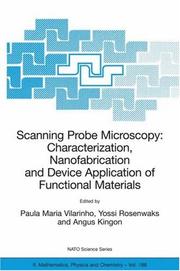
ISBN: 1402030177 1402030185 9786610263707 1280263709 1402030193 Year: 2005 Volume: 186 Publisher: Dordrecht ; New York : Kluwer Academic,
Abstract | Keywords | Export | Availability | Bookmark
 Loading...
Choose an application
- Reference Manager
- EndNote
- RefWorks (Direct export to RefWorks)
As the characteristic dimensions of electronic devices continue to shrink, the ability to characterize their electronic properties at the nanometer scale has come to be of outstanding importance. In this sense, Scanning Probe Microscopy (SPM) is becoming an indispensable tool, playing a key role in nanoscience and nanotechnology. SPM is opening new opportunities to measure semiconductor electronic properties with unprecedented spatial resolution. SPM is being successfully applied for nanoscale characterization of ferroelectric thin films. In the area of functional molecular materials it is being used as a probe to contact molecular structures in order to characterize their electrical properties, as a manipulator to assemble nanoparticles and nanotubes into simple devices, and as a tool to pattern molecular nanostructures. This book provides in-depth information on new and emerging applications of SPM to the field of materials science, namely in the areas of characterisation, device application and nanofabrication of functional materials. Starting with the general properties of functional materials the authors present an updated overview of the fundamentals of Scanning Probe Techniques and the application of SPM techniques to the characterization of specified functional materials such as piezoelectric and ferroelectric and to the fabrication of some nano electronic devices. Its uniqueness is in the combination of the fundamental nanoscale research with the progress in fabrication of realistic nanodevices. By bringing together the contribution of leading researchers from the materials science and SPM communities, relevant information is conveyed that allows researchers to learn more about the actual developments in SPM applied to functional materials. This book will contribute to the continuous education and development in the field of nanotechnology.
Materials --- Scanning probe microscopy --- Matériaux --- Microscopie à sonde à balayage --- Microscopy --- Congresses. --- Congresses --- Microbiologie --- Congrès --- Materials - Microscopy - Congresses. --- Scanning probe microscopy. --- Atomic Physics --- Materials Science --- Physics --- Chemical & Materials Engineering --- Engineering & Applied Sciences --- Physical Sciences & Mathematics --- Scanning electron microscopy --- Matériaux --- Microscopie à sonde à balayage --- Congrès --- EPUB-LIV-FT LIVPHYSI SPRINGER-B --- Scanned probe microscopy --- Physics. --- Condensed matter. --- Optical materials. --- Electronic materials. --- Nanotechnology. --- Thin films. --- Condensed Matter Physics. --- Optical and Electronic Materials. --- Surfaces and Interfaces, Thin Films. --- Surfaces. --- Electron microscopy --- Surfaces (Physics). --- Surface chemistry --- Surfaces (Technology) --- Molecular technology --- Nanoscale technology --- High technology --- Optics --- Materials—Surfaces. --- Films, Thin --- Solid film --- Solid state electronics --- Solids --- Coatings --- Thick films --- Electronic materials --- Condensed materials --- Condensed media --- Condensed phase --- Materials, Condensed --- Media, Condensed --- Phase, Condensed --- Liquids --- Matter --- Surface phenomena --- Friction --- Surfaces (Physics) --- Tribology --- Surfaces

ISBN: 1280337621 9786610337620 3540273085 3540232362 Year: 2005 Publisher: Berlin ; Heidelberg : Springer,
Abstract | Keywords | Export | Availability | Bookmark
 Loading...
Choose an application
- Reference Manager
- EndNote
- RefWorks (Direct export to RefWorks)
This volume focuses on the characterization of nano-optical materials and optical-near field interactions. It begins with the techniques for characterizing the magneto-optical Kerr effect and continues with methods to determine structural and optical properties in high-quality quantum wires with high spatial uniformity. Further topics include: near-field luminescence mapping in InGaN/GaN single quantum well structures in order to interpret the recombination mechanism in InGaN-based nano-structures; and theoretical treatment of the optical near field and optical near-field interactions, providing the basis for investigating the signal transport and associated dissipation in nano-optical devices. Taken as a whole, this overview will be a valuable resource for engineers and scientists working in the field of nano-electro-optics.
Electrooptics. --- Nanotechnology. --- Near-field microscopy. --- Near-field optical microscopy --- Near-field scanning microscopy --- Near-field scanning optical microscopy --- NSOM (Microscopy) --- Scanning near-field optical microscopy --- SNOM (Microscopy) --- Scanning probe microscopy --- Molecular technology --- Nanoscale technology --- High technology --- Electro-optics --- Optics --- Optics, Lasers, Photonics, Optical Devices. --- Quantum Optics. --- Lasers. --- Photonics. --- Quantum optics. --- Photons --- Quantum theory --- New optics --- Light amplification by stimulated emission of radiation --- Masers, Optical --- Optical masers --- Light amplifiers --- Light sources --- Optoelectronic devices --- Nonlinear optics --- Optical parametric oscillators

ISBN: 1280411988 9786610411986 3540268456 3540210504 Year: 2005 Publisher: Berlin ; Heidelberg ; New York : Springer,
Abstract | Keywords | Export | Availability | Bookmark
 Loading...
Choose an application
- Reference Manager
- EndNote
- RefWorks (Direct export to RefWorks)
This unique monograph series "Progress in Nano-Electro Optics" reviews the results of advanced studies of electro-optics on the nanometric scale. This third volume covers the most recent topics of theoretical and experimental interest including classical and quantum optics, organic and inorganic material science and technology, surface science, spectroscopy, atom manipulation, photonics, and electronics. Each chapter is written by one or more leading scientists from the relevant field. Thus, high-quality scientific and technical information is provided to scientists, engineers, and students engaged in nano-electro optics and nanophotonics research. The first two volumes addressed the "Basics and Theory of Near Field Optics" (2002) and "Novel Devices and Atom Manipulation" (2003).
Physics. --- Quantum optics. --- Electronics. --- Microelectronics. --- Optics, Lasers, Photonics, Optical Devices. --- Electronics and Microelectronics, Instrumentation. --- Quantum Optics. --- Electrooptics. --- Nanotechnology. --- Near-field microscopy. --- Near-field optical microscopy --- Near-field scanning microscopy --- Near-field scanning optical microscopy --- NSOM (Microscopy) --- Scanning near-field optical microscopy --- SNOM (Microscopy) --- Scanning probe microscopy --- Molecular technology --- Nanoscale technology --- High technology --- Electro-optics --- Optics --- Electrical engineering --- Physical sciences --- Lasers. --- Photonics. --- Photons --- Quantum theory --- Microminiature electronic equipment --- Microminiaturization (Electronics) --- Electronics --- Microtechnology --- Semiconductors --- Miniature electronic equipment --- New optics --- Light amplification by stimulated emission of radiation --- Masers, Optical --- Optical masers --- Light amplifiers --- Light sources --- Optoelectronic devices --- Nonlinear optics --- Optical parametric oscillators

ISBN: 1280745223 9786610745227 3540286810 3540286659 Year: 2005 Publisher: Berlin ; New York : Springer,
Abstract | Keywords | Export | Availability | Bookmark
 Loading...
Choose an application
- Reference Manager
- EndNote
- RefWorks (Direct export to RefWorks)
Focusing on nanophotonics, which has been proposed by M. Ohtsu in 1993, this volume begins with theories for operation principles of characteristic nanophotonic devices and continues with novel optical near field phenomena for fabricating nanophotonic devices. Further topics include: unique properties of optical near fields and their applications to operating nanophotonic devices; and nanophotonic information and communications systems that can overcome the integration-density limit with ultra-low-power operation as well as unique functionalities. Taken as a whole, this overview will be a valuable resource for engineers and scientists working in the field of nano-electro-optics.
Electrooptics. --- Nanotechnology. --- Near-field microscopy. --- Near-field optical microscopy --- Near-field scanning microscopy --- Near-field scanning optical microscopy --- NSOM (Microscopy) --- Scanning near-field optical microscopy --- SNOM (Microscopy) --- Scanning probe microscopy --- Molecular technology --- Nanoscale technology --- High technology --- Electro-optics --- Optics --- Engineering. --- Optics, Lasers, Photonics, Optical Devices. --- Quantum Optics. --- Engineering, general. --- Construction --- Industrial arts --- Technology --- Lasers. --- Photonics. --- Quantum optics. --- Photons --- Quantum theory --- New optics --- Light amplification by stimulated emission of radiation --- Masers, Optical --- Optical masers --- Light amplifiers --- Light sources --- Optoelectronic devices --- Nonlinear optics --- Optical parametric oscillators
| Listing 1 - 10 of 11 | << page >> |
Sort by
|

 Search
 Feedback
 About UniCat
  Help
Help News
News